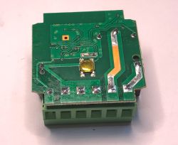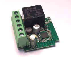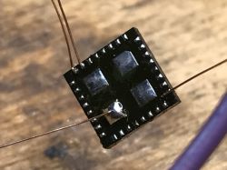
T34 a Wi-Fi and BT combo chip integrating BK7231N core along with crystal, RF matching component, and most other peripheral components within a tiny SMD case. The T34 dimensions are 6±0.1 mm (W) × 6±0.1 mm (L) × 0.85±0.1 mm (H). This reduces the size required on the board and saves manufacturing cost.
Internally, T34 is compatible with BK7231N firmware, so it can be flashed with OpenBeken.
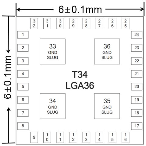
But first, let's consider T34 pins:
| Pin No. | Symbol | I/O type | Description | 1, 3, 32, 33, 34, 35, and 36 | GND | P | Ground pins. 33, 34, 35, and 36 are the ground pads at the back of the chip. | 2 | ANT | I/O | External antenna with 2.4 GHz RF input and output. | 4 and 5 | VCCPA | P | RF PA power input. Voltage range: 3.0V to 3.6V. And 3.3V power supply is recommended. | 6 | VDDDIG | O | Digital power output. The voltage is about 1.2V. | 7 | VDDAON | O | Normally open power output. The voltage is about 1.2V. | 8 | VBAT | I | Chip main-power input. Voltage range: 3.0V to 3.6V. And 3.3V power supply is recommended. | 9 | CEN | I | The CEN pin of the chip, without a reset function. This pin is floating inside the chip. | 10 | P28/ADC4/RXEN | I/O | GPIO or ADC4 or set high during RF reception. | 11 | P14/SD_CLK/SCK/ANT0 | I/O | GPIO, or CLK of SD, or SCK of SPI, or Bluetooth LE antenna control ANT0. | 12 | P16/SD_CMD/MOSI/ANT2 | I/O | GPIO, or CMD of SD, or MOSI of SPI, or Bluetooth LE antenna control ANT2. | 13 | P15/CSN/ANT1 | I/O | GPIO, or CSN of SPI, or Bluetooth LE antenna control ANT1. | 14 | P17/SD_D0/MISO/ANT3 | I/O | GPIO, or D0 of SD, or MISO of SPI, or Bluetooth LE antenna control ANT3. | 15 | P26/ADC1/IRDA/PWM5 | I/O | GPIO, or ADC1, or IR receiver or PWM5. | 16 | P24/ADC2/LPO_CLK/PWM4 | I/O | GPIO, or ADC2, or low power clock 32.768K output, or PWM4. | 17 | P23/ADC3/TDO/F_SO | I/O | GPIO, or ADC3, or JTAG TDO, or flash data output when downloading with SPI. | 18 | P22/ADC5/CLK_26M/TDI/TXEN/F_SI | I/O | GPIO, or ADC5, or crystal frequency output, or JTAG TDI, or set high during RF transmission, or flash data input when downloading with SPI. | 19 | P21/ADC6/I2C1_SDA/TMS/F_CSN | I/O | Mode selection pin for selecting RF test firmware or app firmware. Pulling down this pin will enter the RF test mode. | 20 | P20/I2C1_SCL/TCK/F_SCK | I/O | GPIO, or SCL of I2C1, or TCK of JTAG, or the clock when flash is downloaded by SPI. | 21 | P6/CLK13M/PWM0 | I/O | GPIO, or 1, 2, 4, and 8 frequency division output of crystal clock, or PWM0. | 22 | P7/WIFI_ACTIVE/PWM1 | I/O | GPIO, or WIFI_ACTIVE control when Wi-Fi and Bluetooth coexist, or PWM1. | 23 | P8/BT_ACTIVE/PWM2 | I/O | GPIO, or BT_ACTIVE control when Wi-Fi and Bluetooth coexist, or PWM2. | 24 | P9/BT_PRIORITY/PWM3 | I/O | GPIO, or BT_PRIORITY control when Wi-Fi and Bluetooth coexist, or PWM3. | 25 | P10/DL_RX/UART1_RXD | I/O | GPIO, or RXD when downloading flash with UART, or RXD of serial port UART1. | 26 | P11/DL_TX/UART1_TXD | I/O | GPIO, or TXD when downloading flash with UART, or TXD of serial port UART1. | 27 | P1/UART2_RXD/I2C2_SDA | I/O | GPIO, or RXD of serial port UART2, or SDA of I2C2. P1 is used for self-calibration and cannot be used for other functions. | 28 | P0/UART2_TXD/I2C2_SCL | I/O | GPIO, or TXD of serial port UART2, or SCL of I2C2. | 29 | XI | I | T34 has a built-in crystal, and no external crystal is required. | 30 | XO | O | T34 has a built-in crystal, and no external crystal is required. | 31 | VSYS | O | System power output. Voltage range: 2.7V to 3.0V. |
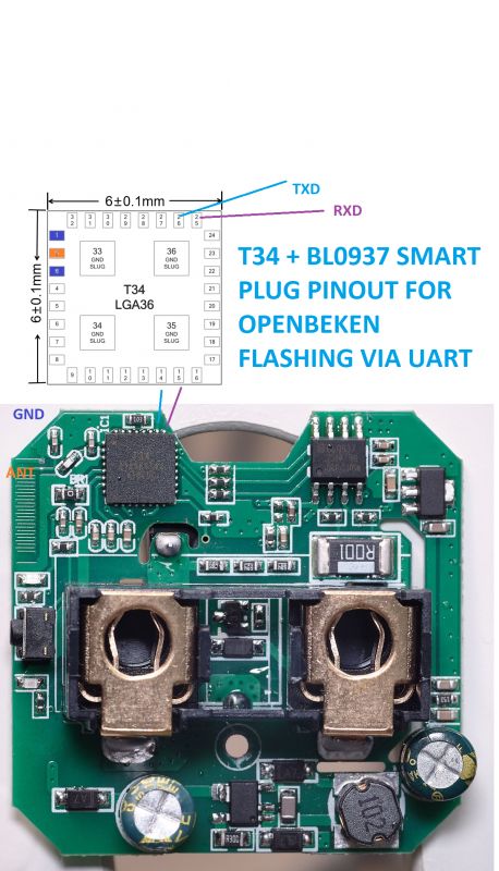
For flashing, you just need TX1, RX1 and power (GND and 3.3V).
T34 datasheet:
In the next section, I'll present and flash a sample T34 device, so it can run free from the cloud and be paired with Home Assistant.
LSPA9 plug with T34
I've bought a very common plug on Aliexpress, which is sold for about 5$:
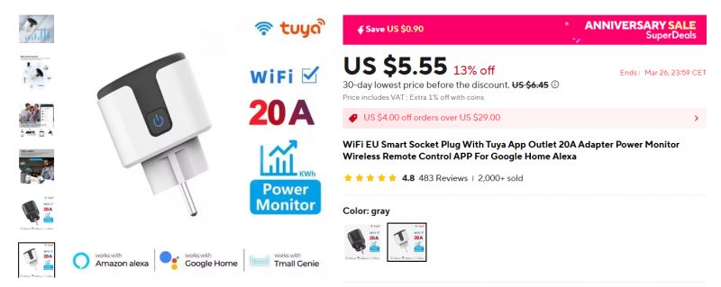
Plug is branded as QNCX.
It arrived fairly quickly:
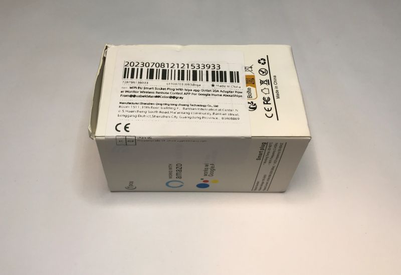
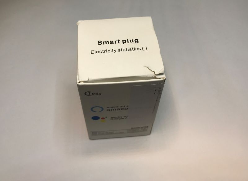
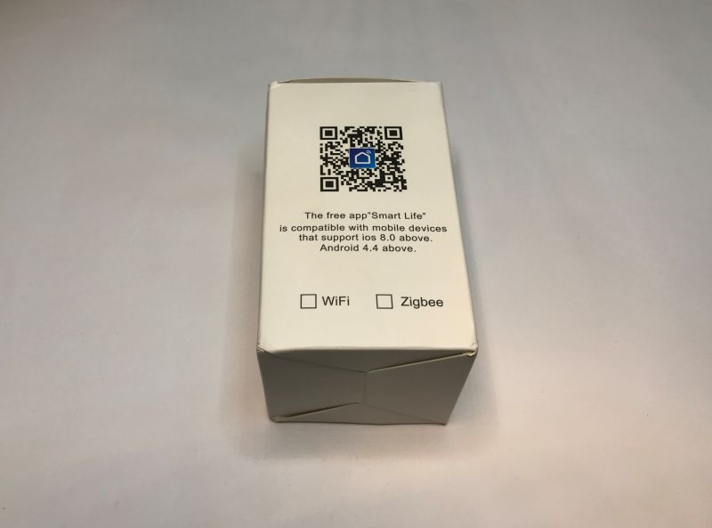
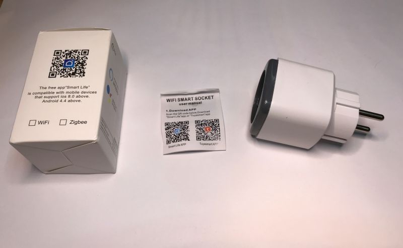
The device can be opened with vice or by prying, it may be sometimes hard or easy, it depends on how much glue manufacturer used.
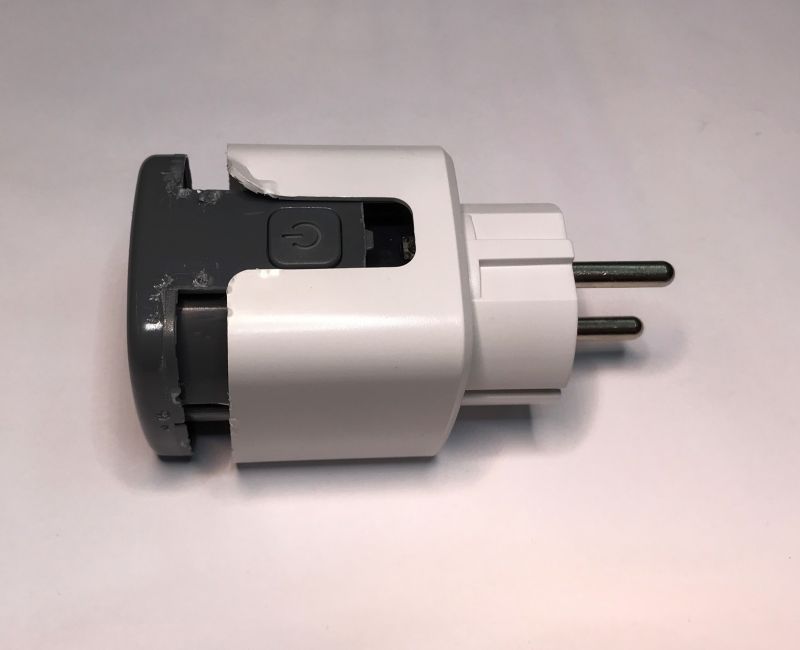
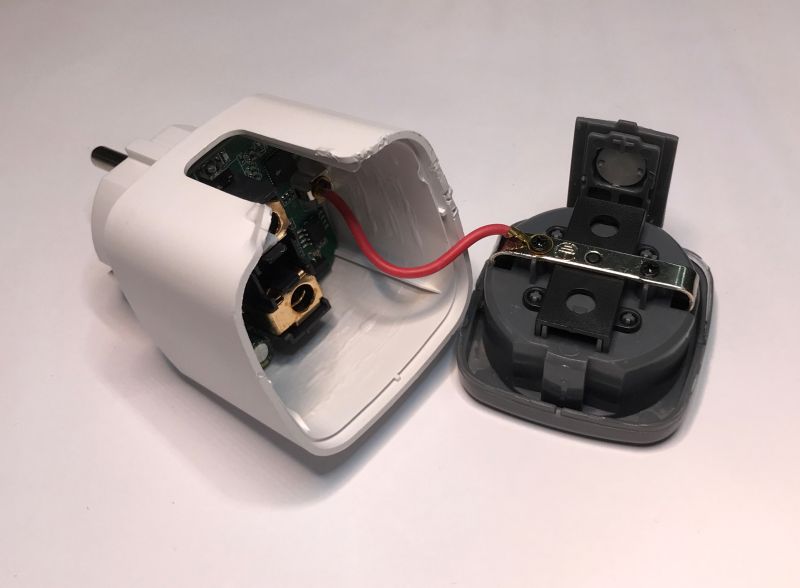
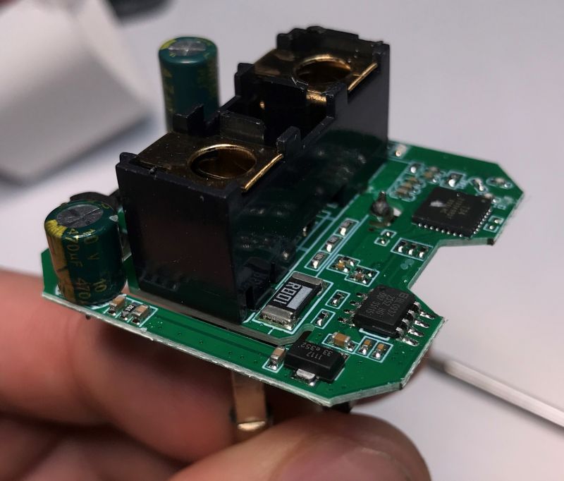
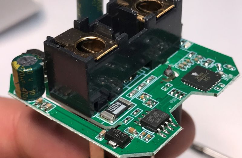
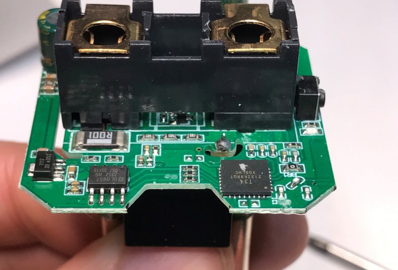
There is a single board inside, it can be removed by unscrewing one screw:
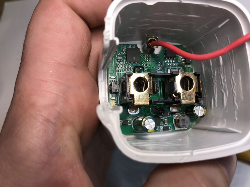
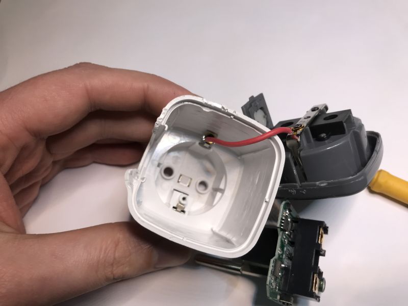
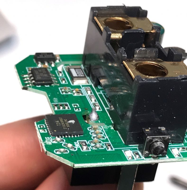
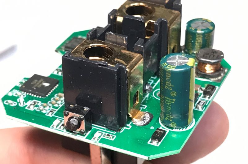
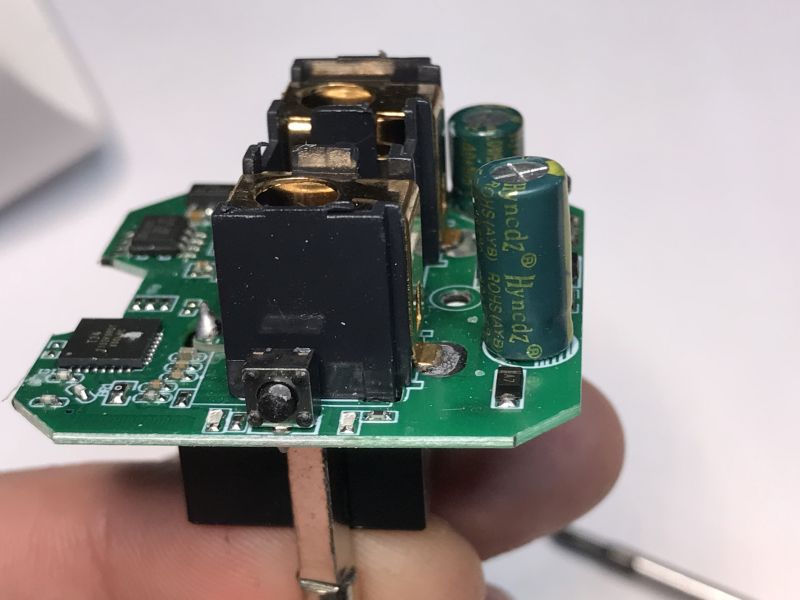
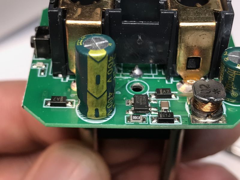
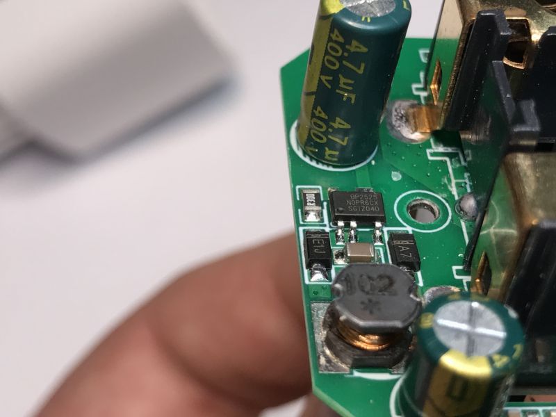
The device is using T34 chip along with BL0937 for power metering. Futhermore, there is a step down power supply based on BP2525 and a 3.3V LDO to get 3.3V for the WiFi chip.
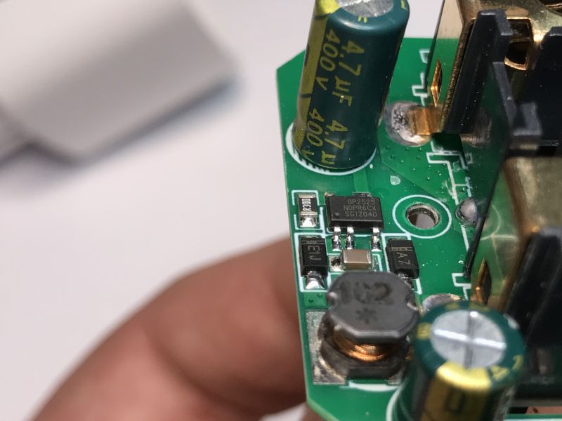
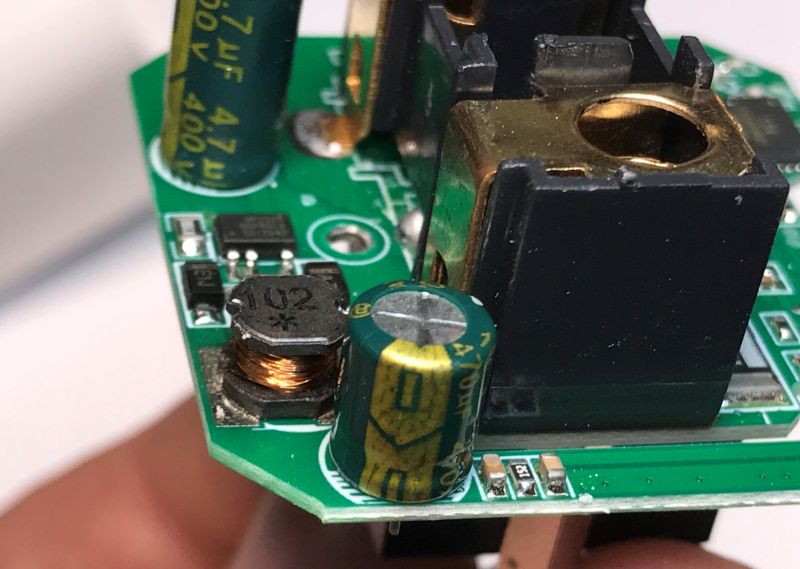
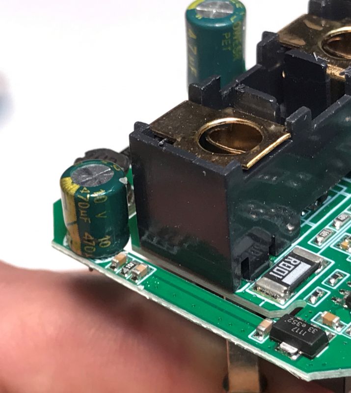
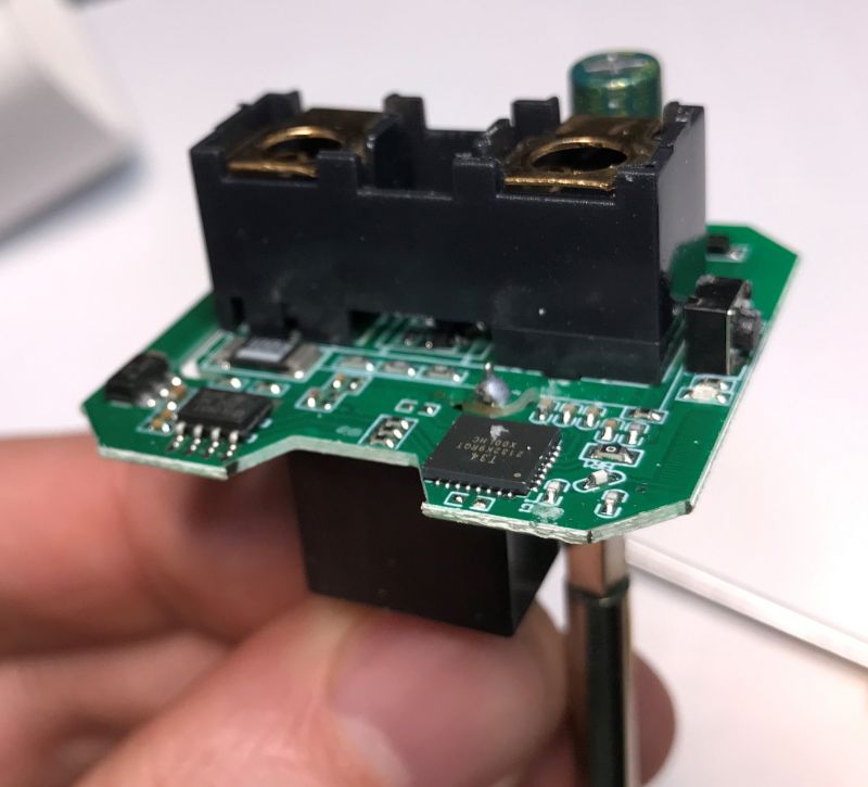
Flashing attempt - how not to flash
There are no RX/TX pads, but one of UART signals is routed to small SMD resistor pad. I've wanted to use this, as shown on image below:
However, I've made a small mistake and used too large wires:
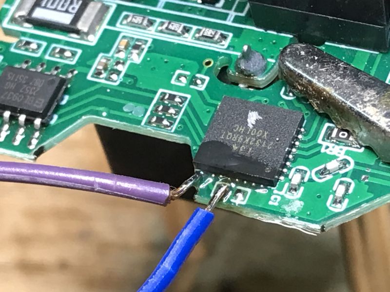
Ultimately, one of the pads fell off and I had to take a different approach.
So, if you are attempting this, use thinner wires! Like this:
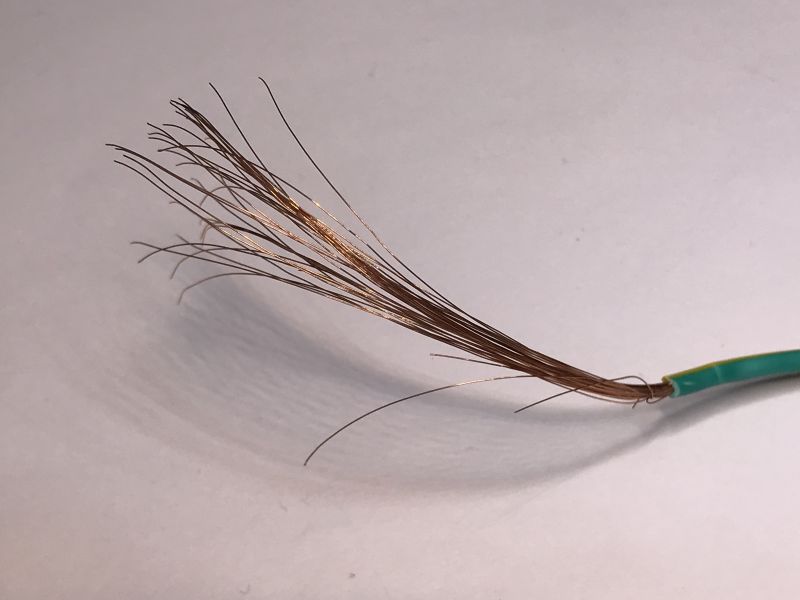
Second flashing method
And so, I had to remove the T34 from the board with hot air. I added some extra flux and lowered the air flow to avoid affecting nearby components.
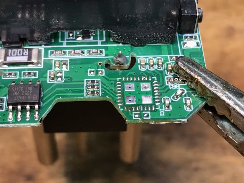
Here you can see the pad that I damaged (not the resistor pad, but the tiny pad of the other UART pin):
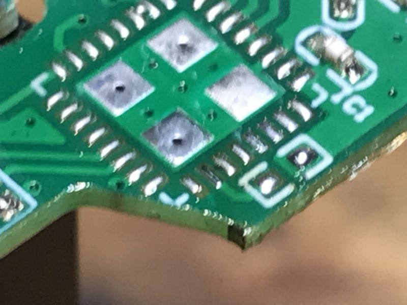
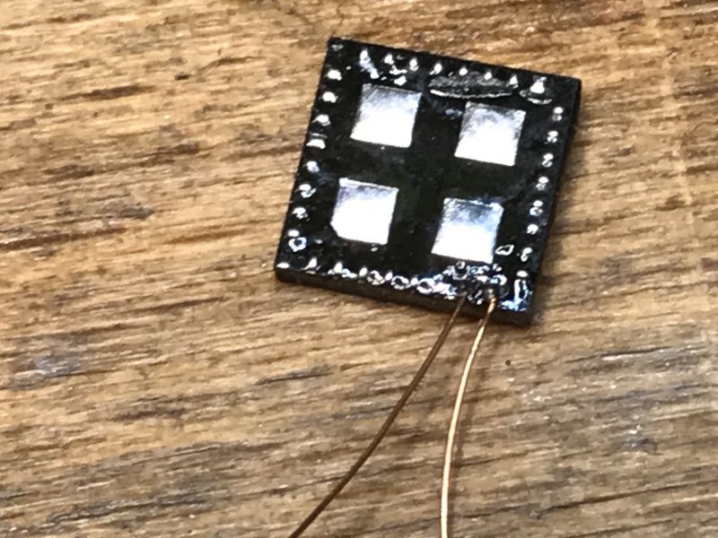
Then I decided to solder directly to QFN pads, but this time I used thin wires:

It is also recommended to secure them in place with some hot glue or sticky tape, because it's still very easy to tear the pad.
Here's UART soldered:
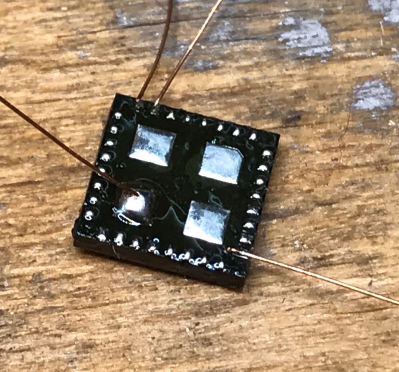
And then ground (large pad) and power (3.3V):
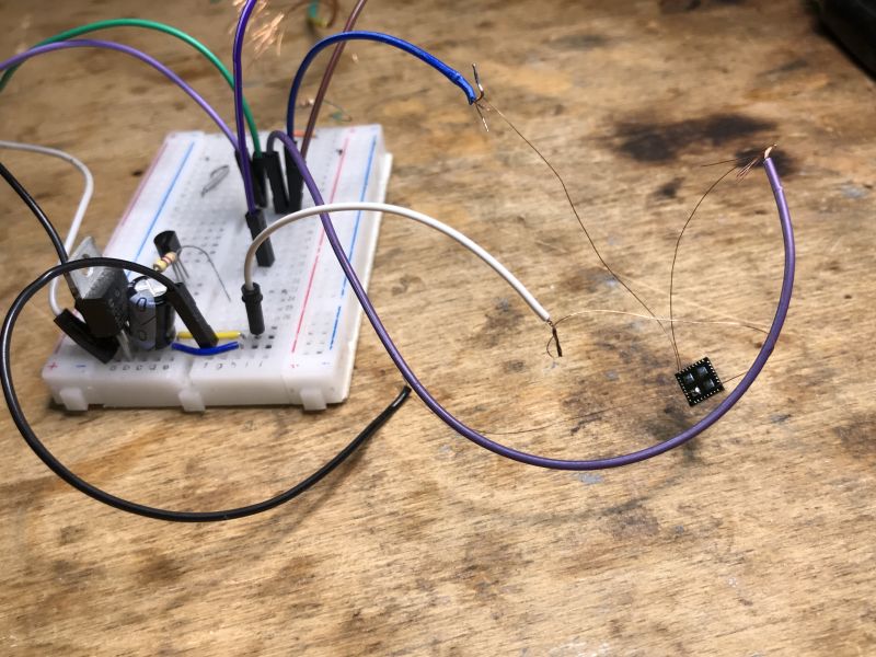
Full circuit:
For flashing, I've used our GUI tool:
https://github.com/openshwprojects/BK7231GUIFlashTool
This is how I performed the power on/off cycle:
Sadly it's not possible to check if WiFi access point is available after flashing. That's why I decided to solder it back in place without doing extra checks.
I cleared up the T34 pads with flux and solder wick. Then I added flux on the PCB and decided to reuse the solder that was already there.
After a brief heating, with a small air flow, the module has slightly moved itself in place and seated itself correctly. I had no corrections to do myself.
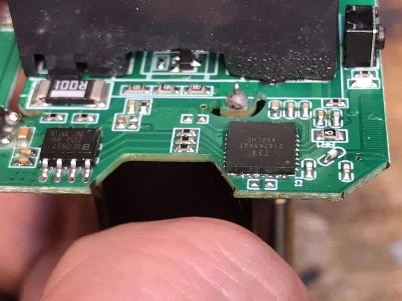
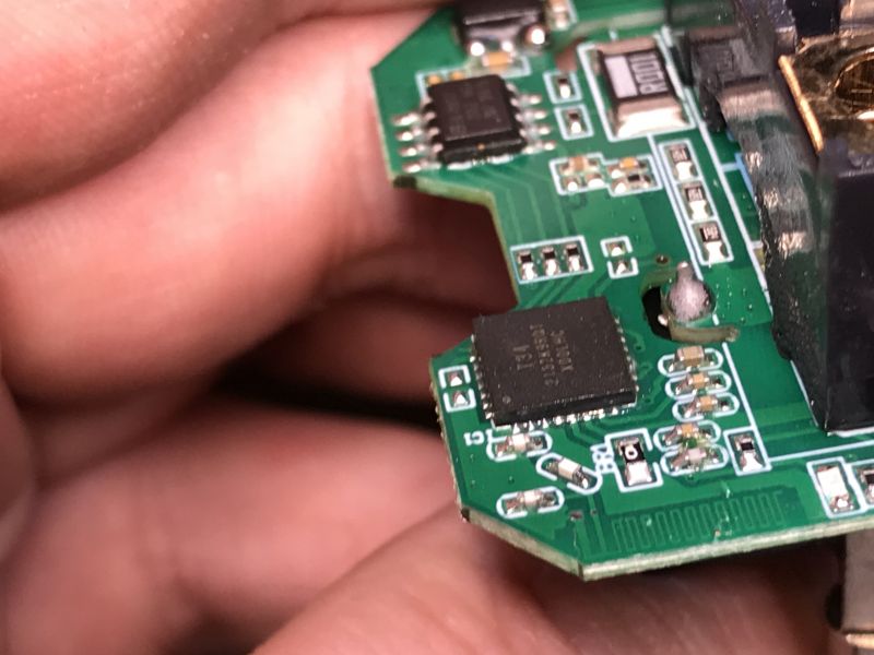
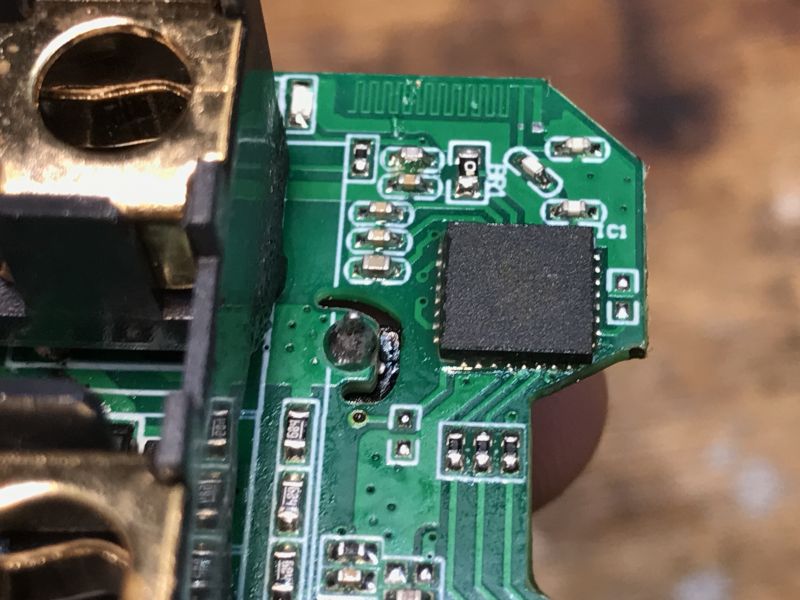
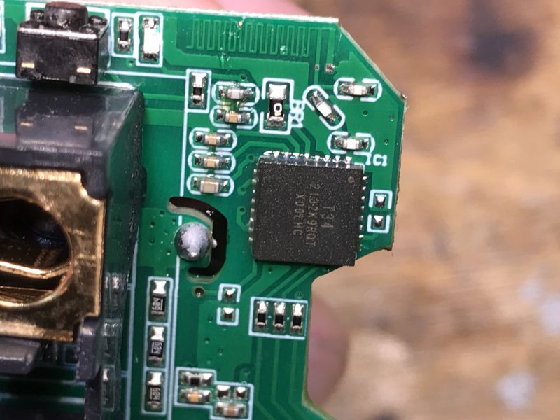
Luckily the soldering turned out to be very easy and device worked at the first try.
I've used template from here: https://www.elektroda.com/rtvforum/topic4042412.html#21030449
Everything is working correctly.
Factory flash backup:
https://github.com/openshwprojects/FlashDumps/commit/9b564848c33a9622df7f94ed19855831ec574040
Summary
New devices with T34 devices are still certainly flashable, you can do that just like you'd flash BK7231N.
This particular plug can be still flashed without desoldering T34, you don't even need hot air, just a cheap soldering iron, but don't repeat my mistake and use a very thin wires to access UART TX and RX. Then you can just feed either 5V to the input of AMS1117-3.3V or 3.3V to the output and it will flash just fine.
Otherwise you'll need to desolder T34 chip with hot air. It's still possible and in my opinion it's actually way more easy than it seems. Soldering to T34 pads is also relatively easily, as long as you use flux and a correct type of wire. Just don't apply force or you'll rip them too. It may be safer to secure T34 wires in place with some hot glue to avoid pulling them accidentally.
Soldering T34 back is also easy, I just cleared T34 pads with soldering wick and added flux to the board, I didn't even clean the old solder. Old solder melted just fine. I will try to make a video with it soon, but that's for another topic.
So, summing up, T34 devices are still flashable and it's still possible to do it in most cases even without hot air.
Did you encounter any T34 devices so far? Let us know! We can help you with running your devices 100% local, without the cloud and with Home Assistant.
Cool? Ranking DIY Helpful post? Buy me a coffee.


